RetroChallenge 2023/10 - Applix1616 restoration/documentation

So, during October, I’m going to try restoring an Applix1616 to working condition. The system came into my possession from a Canberra local that was clearing stuff out of his house and offered it up to people at the local makerspace (Make Hack Void). He did not remember how it came into his possession or from whom. Of course, I snapped it up.

The Applix1616 was an Australian kit computer with a Motorola MC68000 CPU from 1986, made by Applix Pty Ltd in NSW. Applix was started by Paul Berger and Andrew Morton (aka akpm, who later became a maintainer of the Linux kernel). The design for the machine, plus some articles on construction and testing, appeared in Electronics Today International with a series of articles starting in December 1986.

If you want to read more on this, here’s some links:

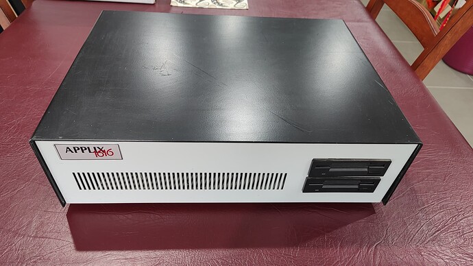
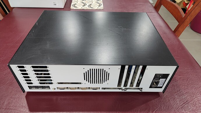
Below is the state of the machine when I received it.

Front:

Back:

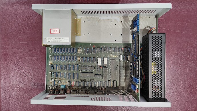
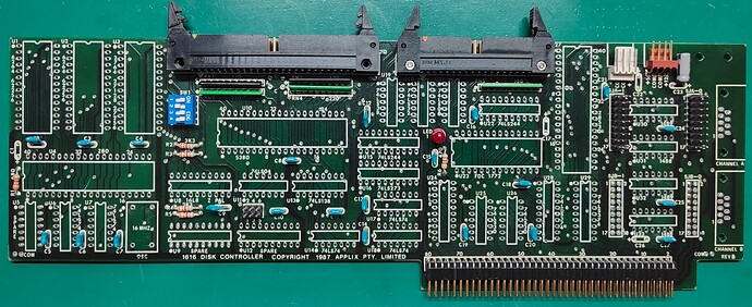
Inside, with one Disk IO Controller installed:

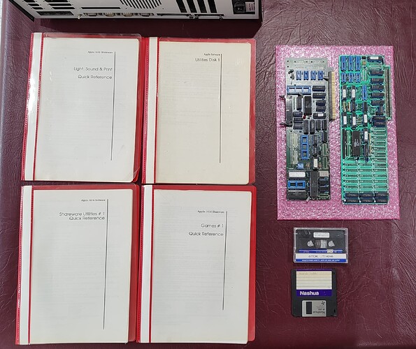
Manuals/Disks, plus the 2 extra cards:

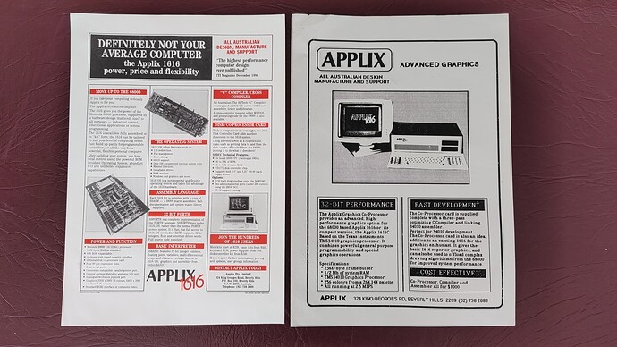
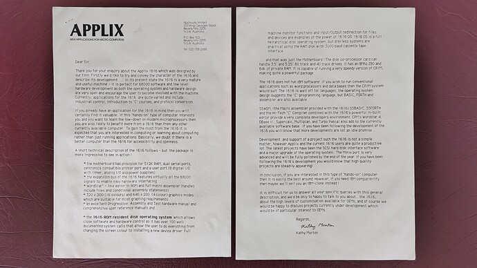
Since then, I received a few more related paper docs that the previous owner found.

Ad copy:

System enquiry response:

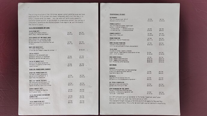
Price list:

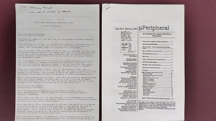
Copy of preliminary Minix - 1616 document, along with a copy of uPeripheral (Applix 1616 users newsletter):

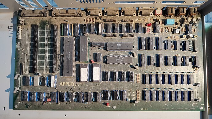
Since then, I have disassembled the machine from its case and cleaned the tops of all the chips on the mainboard. This was so I can document all the modifications (aka bodge wires) that have been done to the base motherboard, plus figure out what I might need as part of the restoration process (ie: to avoid delivery delays where possible). I also checked for any corrosion, as I wasn’t going to wait around till October to treat corrosion if it was just going to get worse. Fortunately there are no batteries anywhere in this machine.

Note that I have not tested the power supply, nor have I attempted to power up the machine or test the floppy drives. No other work has been done.

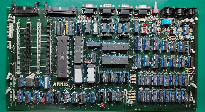
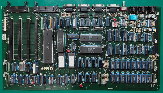
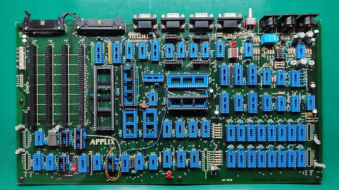
Motherboard with the chip tops cleaned:

Rough plan for October (what I’m setting out to achieve and document here):

  • Document fully the bodge wires on this machine and try to figure out the reason they’re present (eg: broken traces, circuitry revision, upgrades, etc).
  • Clean the board, plus remove all chips and current bodge wires from the board. Check for any bad joints, etc.
  • Remove/test/replace the electrolytic capacitors on the mainboard.
  • Confirm separate operation of the power supply and restore if possible. Will use an ATX break-out board if this delays anything. The mainboard requires +12V, +5V, -12V and -5V, which the break-out board I have provides.
  • Where practical, test all chips on the board (using a Chip Tester Pro from BackBit.io). This will definitely not include the MC68000 as the Chip Tester doesn’t support it.
  • Take ROM images and PAL/GAL images (where possible) from the machine for archival purposes using the Chip Tester Pro.
  • Follow the build and test process documented in the “ETI project 1616 Hardware and Construction-Manual” (available on Eric Lindsay’s site, plus from the Hackaday.io Applix1616 Documentation project), which guides you through what chips to insert where, and what signals to look for, etc.
  • Confirm working operation (OS is in ROM).
  • Scan all the paper documents that came with the machine for base level archival purposes.

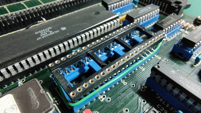
FWIW: When reinstalling chips that currently have bodge wires directly attached to lifted pins, where possible I will install them in machine sockets and tap the pin off separately, unless they can be safely pulled from an existing trace or have been confirmed that they aren’t needed (eg: fixing a broken trace/via). This idea is inspired by an existing mod on the machine, which adds a bodge wire and a resistor pull-up pack to a machine socket under the R6522AP, located to the right of the the MC68000. Fortunately all the IC pins that have been lifted to have bodge wires attached are intact.

Bonuses if I can get them:

  • Document, test and confirm operation of the at least one of the Disk Controller boards, and clean/test the NEC floppy drives. If possible, get ZR-DOS working on the Disk Controller (depends what is on the disks and in ROM).
  • Document, test and confirm operation of the RAM Expansion board.
  • Add a 3rd Expansion socket to the mainboard (currently 2 of 4 are populated).
  • Populate extra parts on at least one of the Disk Controller boards to enable the 2 extra serial ports.
  • Get a working SCSI hard disk set up (using a BlueSCSI V2).
  • Extract data from the cassette tape and disk that came with the machine.
  • if possible, update the OS in ROM to the last revision known (V4.7a).

FWIW: The Disk Controller has a Z80 on it that can run a port of ZR-DOS (passing the UI back to the MC68000), effectively allowing the machine to offload disk operations from the MC68000. The Disk Controller also has a SCSI bus, but this too is hooked to the Z80, so disk access using that SCSI controller is slow, but apparently possible via ZR-DOS. The RAM Expansion board has a SCSI controller directly mapped to the MC68000 bus, so I’ll be planning to use that SCSI bus where possible.

Note: I’ve documented the above state of the machine, as I don’t want to claim what I’ve done already as part of the RetroChallenge work. It’s not a huge amount, but it’s not wholly insignificant.
4 Likes

Hi Cefiar, if you need more documentation or software for the Applix, we have a huge Repository at Discussion Forum for all things Microbee of Manuals, Newsletters, Brochures, Schematics, ROMs and about 150 disks of Software for the Applix 1616.

4 Likes

Hi ChickenMan!

I was somewhat aware of that forum and the repository, but it reminded me to get off my rear and actually register for it. Thank you. I am VERY SURE that it’ll be useful. :smiley:

1 Like

So, first day actually working on the machine as such.

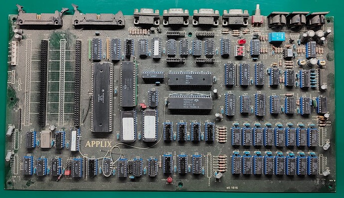
Took the motherboard out, grabbed some pics (both sides) and then gave it a clean to remove all the dust. Before cleaning I made sure to take close up pics of the bodge wires, the switch settings, and all the jumper headers. the board is a Rev B board, which may prove relevant later, particularly for things like the bodge wires.

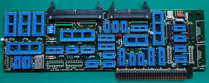
Top of the motherboard (pre-cleaning):

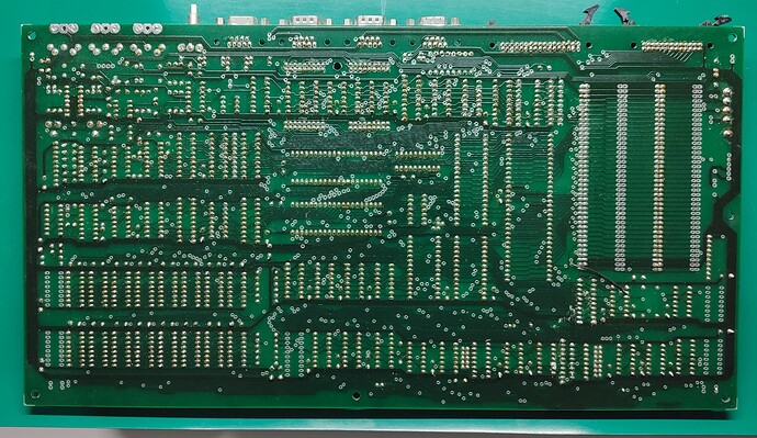
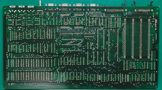
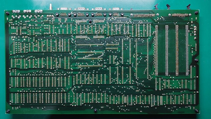
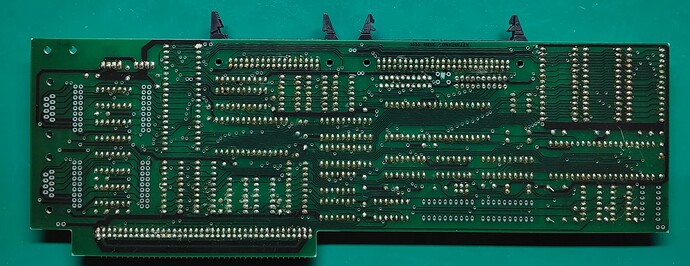
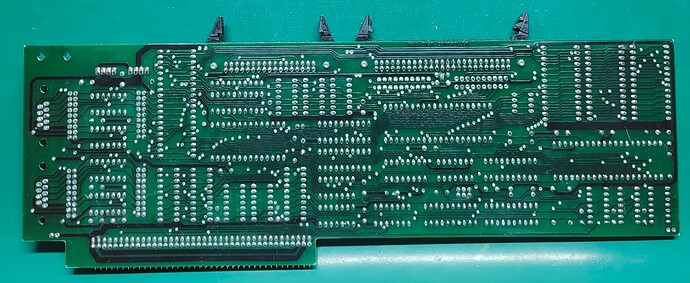
Bottom of the motherboard:

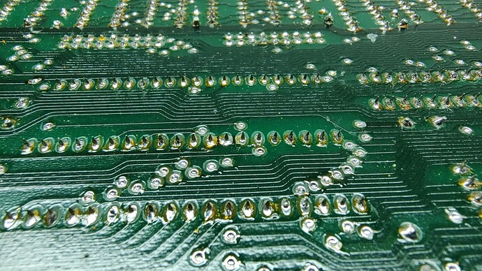
The solder work on the bottom is pretty good considering this is a kit computer. Probably can do with a clean to remove all the flux, but that’s for another day.

Post first round of cleaning:

There’s a few bits I’ve cleaned since, but some of the dust really wants to hang around. I’ll give it a better clean when I do the bottom of the board.

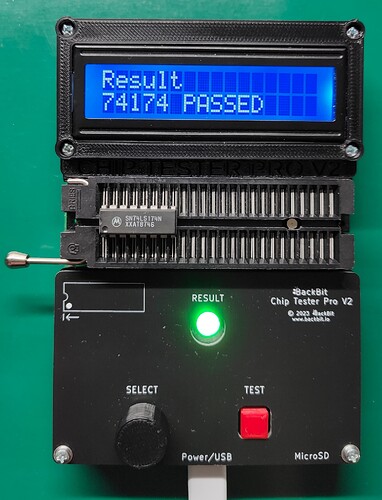
Took out a bunch of chips and ran them through the ChipTester Pro V2.

74LS174 in the tester:

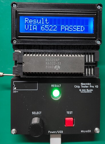
Rockwell 6522 in the tester:

I’ve tested most of the 74-series and all the 4000 series chips in the machine and they all passed. Also as shown, I tested the Rockwell 6522.

While I had the 6522 out, here’s a close up pic of the 4 pull-down resistors that are on the 6522 Address bus (A0-A3, which are pins 35 thru 38).

Machined socket with a resistor pack attached to 4 pins and bodge wire going to ground on the 6522:

The chips I have NOT tested so far:

  • All the 74 series chips that are connected by bodge wires.
  • MC68000 - The CPU.
  • Rockwell 6545 - Video Controller.
  • Zilog 8530 - Serial Communications Controller.
  • LM817, LM301 & LM319 - Op Amps (audio/tape).
  • DAC0800 - 8 Bit DAC (audio).
  • MC1488/MC1489 - Serial transceiver chips.
  • GM71256’s - Ram.
  • PAL1 and PAL2 - Programmable logic gates.

As part of the testing, I ripped the contents of the 27C512 EPROMS. The binary contents don’t match any of the Rom versions I’ve found online (which doesn’t include binaries for the last Rom released; V47a).

Did some investigating and the bodge wires are a combination of fixes for common issues (eg: the pull-downs on the R6522) and the 15 Mhz speed upgrade .

Next steps:

  • Test Ram (appears to be supported by the tester).
  • Remove all the bodge wires and test all the remaining 74 series chips.
  • Rip the PALs.
  • Re-implement the bodge wires using machined IC sockets.
  • Check and test power supply (separately).
1 Like

Looks like an awesome project! Please sign up for the RetroChallenge so we can consider your hard work when we award prizes:
RC2023/10 Sign up

1 Like

Thanks for reminding me to register epooch!

So, made some more progress.

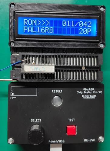
Ripped TPAL (PAL1) and VPAL (PAL2). The TPAL is V2 (timing, related to the 15 Mhz mod), while the VPAL is V5.

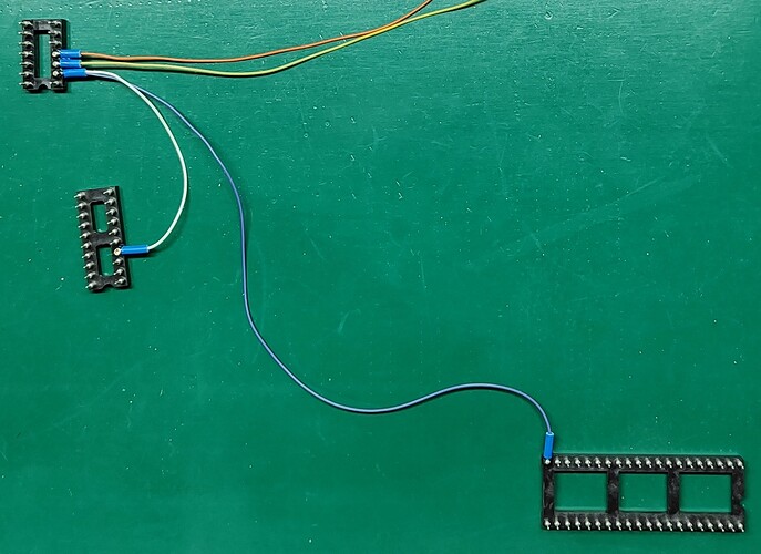
Didn’t want to bend the pin on the TPAL yet, so used a bodge wire to connect the upturned pin to the Chip Tester for ripping:

Tested Ram & LM319. All passed!

Cleaned the top and bottom of the case. Also replaced standoff screws with nylon ones and added in 2 extra nylon standoffs that were the same height around slot area to support the motherboard when cards are installed/removed.

  • One of the nylon standoffs does not screw through the board, but sits between Slot 3 and the MC68000. It’s the one in the middle, just to the right of the rear card slots. There was already a hole in the case, but it doesn’t line up with a matching hole in the board, so using a nylon standoff provides support without causing an issue by shorting something out.
  • Plan to use the replaced screws elsewhere, since a number of screws were missing. None of the holes are plated or grounded, and the nylon screws avoid marring the case or the motherboard surface.

The nylon hardware is black, while the original metal hardware ones are nickel coloured:

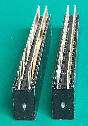
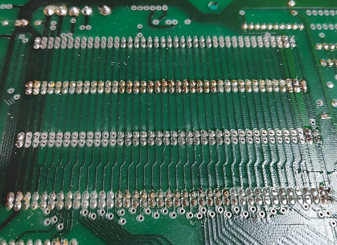
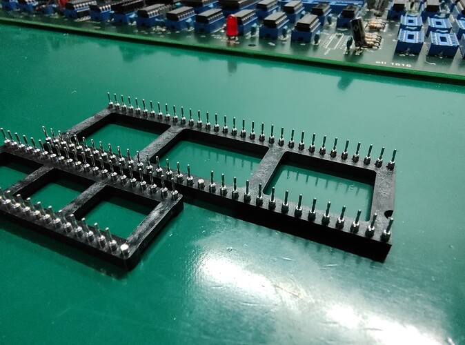
Populated the 2 remaining expansion slot connectors. The 80 pin header connector was no longer available, so had to use 2x 40 pin headers instead. To get them to fit, needed to sand down one end (used 600 grit sandpaper). Also decided to touch up all the existing slot connections while I was at it, since some didn’t seem to have enough solder on them.

Top tip: Sand down the flat end of the connector! Usually one end has an injection moulding mark (where the sprue is). You do not want to sand that end down as it’s not as flat, plus in some cases it’s usually marginally thicker. All of that makes it hard to remove the right amount of plastic from the ends while keeping it square to the rest of the connector.

Pic of sprue end of connector:

Part way thru soldering the connectors:

Added screws/nuts to connectors on the back to avoid bending, as they are on the edge of the board:

  • Joystick/Serial/Video connectors. Metal hex screw on top with plastic nut underneath. M3 hardware.
  • Centronics/User IO port connectors. Metal hex screws with on bottom (with washer), with metal nut on top. M2 hardware (M2.5 would have been better).

Touched up the solder joints for all the edge connectors. While doing the cassette/speaker/keyboard DIN connectors and the power connector, spent the time to make them actually line up a bit, as they were all pointing slightly different directions previously, or not at right angles to the board.

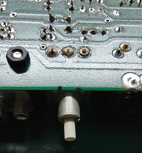
Added more solder to the joints for the reset switch pins, as the switch would move up and down if you touched it. Also bent over the pins over the edge of the board to give it some mechanical rigidity. Usually a design would have these go through solder holes to provide a physical connection to avoid movement.
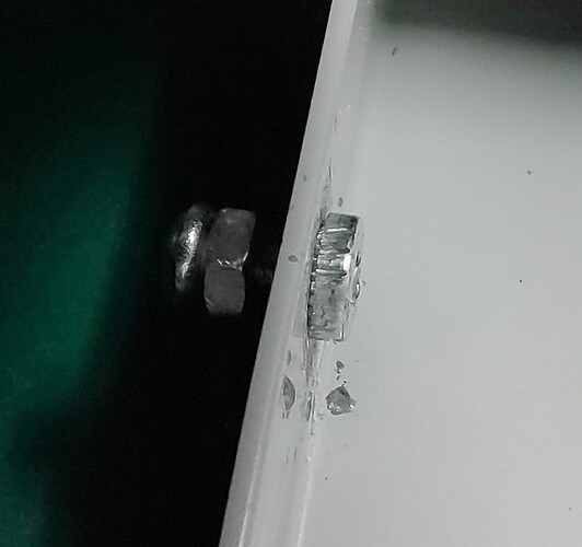
Half way through bending the pins on the switch. Left pin is standard, right pin has been bent, plus you can see the one of the nylon nuts on the bottom of the board for the Joystick connector:

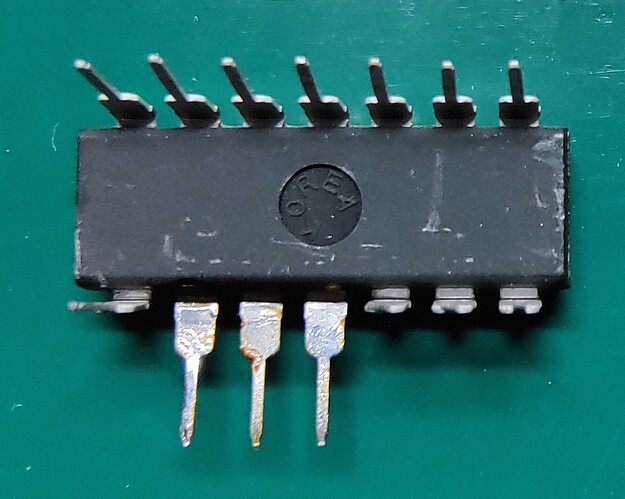
Cleaned up the solder on the 74 series chips that had legs bent for bodge wires, using the 74 series chips as the guinea pigs for this process. Leaving the solder on the pin would make bending them back harder, plus may not allow the chip to sit properly in the new machined sockets. Once I bent down the pins, I put them through the ChipTester Pro. One worked (1 pin re-bent), the other failed (3 pins bent). A bit of cleaning and some testing however revealed that the issue was the old flux (rosin) and the new flux (no clean rosin) together formed a conductive layer! Once cleaned, the failed chip was working again. This means I’m definitely going to need to clean all the flux residue off the board before I attempt power-up.

Solder cleaned up prior to bending the pins back. Make sure to clean solder off both sides, and also any flux:

I’ll probably break out my solder sucker (an electric pump one) and use this to clean the solder off all the bent pins, rather than using solder wick. Fortunately there’s only 2 more chips (MC68000 and R6545), and each of these only has one pin bent. Will replace both the 74 series chips with new, just to avoid any potential issues.
I also tested the power supply and so far it’s working fine, putting out the right voltage on each pin. When you turn it on and turn it off, it emits a tiny low volume high pitched squeal (>16 Khz - I might be in my 50’s but I can still hear that high) for less than half a second. This is from the high frequency switch-mode supply startup/shutdown, so I’m not TOO concerned at this point, but I’ll probably do some more testing, just in case.

I’ve also prepared all the machined sockets to implement the bodge wires. After trimming the pins, I filed them slightly to avoid any possible connection to the socket underneath.

Machined sockets for the R6545 and the MC68000 prepared:

Top of board. Looking much better:

Bottom of board. Looks better but will definitely need to clean off that flux residue:

Things to do next:

  • Solder up all the vias and unpopulated solder holes.
  • Redo a bunch of solder joints on the bottom of the board.
    – Lots of joints here that don’t have enough solder on them. Definitely not the greatest solder job.
  • Clean all the flux residue from the bottom of the board.
    – This is why I’m going to fill in all the vias and solder holes, as otherwise cleaning the bottom will just spread all the flux residue onto the top of the board.
  • Clean and re-bend pins on R6545, MC68000 and TPAL.
  • Implement bodge wires on the machined connectors.
  • Start testing chips on the memory expansion and disk controller boards, plus detail what cleaning/remediation is required.
2 Likes

Didn’t quite get as much done as I wanted, but thought I’d post an update.

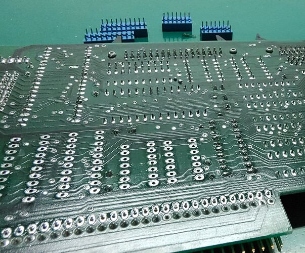
Pulled all the IC’s out of their sockets. Fortunately everything is socketed. Then I filled in the vias and blank pads. Lots and lots of vias. About 2 hrs all up (with regular breaks). Having thin solder (0.35mm) really helps in just adding the right amount to each via/hole.

The 0.35mm solder is my go-to for fiddly jobs, tho I have 0.56mm and 0.8mm on hand for those bigger joins.

Board with vias filled but before cleaning:

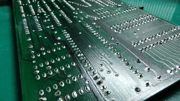
Some of the original joints don’t have enough solder, particularly on ICs. It seems to be a common problem spread across the board - Many are good, some are not quite so good. While these are probably electrically sound, I’ll touch them up after cleaning the board.

Closer pic of some of the sub-par solder joints, plus you can see all the excess flux:

After cleaning the PCB, everything looks MUCH better (used Servisol Electronic Circuit Board Cleaner - NA-1008). There’s still some residue on the board, but I’ll wash the board with isopropyl once I’ve touched up all those sub-par joints. Note that I only cleaned the solder side, as the component side was already fairly clean.

Board after cleaning with Servisol:

Soldering bodge wires to the machine sockets was… somewhat challenging. Having multiple pairs of fine tweezers with different shaped tips/bends helps immensely. I bought extra sockets of each type just in case I made a mistake along the way, though in the end I didn’t need them. Used a different colour for each bodge wire, which helped immensely to ensure that I got all the wires connected to their correct places. To aid in the mechanical stability of the wires where they come off the sockets, I’ve been using a small amount of insulation off some larger wire over where the bodge wires get soldered to the pin of the machine socket. A tiny bit of superglue holds the insulation to the body of the socket, keeping it nice and stable. I didn’t have any heatshrink small enough for the job, something I’ll have to rectify for future restoration work like this.

Soldered 74LS08/TPAL/R6545 socket harness:

To 100% ensure that the shortened ends of the machine sockets don’t touch the normal IC sockets underneath, I used small pieces of a PVC based high temp tape that I’ve had about for a while, to act as a physical barrier. I was going to use Kapton, but I couldn’t find my small roll of it, only the large (200mm wide) one, which would have been even more annoying to deal with. The PVC tape is rated to about 200°C, which given that the joints underneath the sockets shouldn’t need to be soldered again, should be more than ample to the job.

R6545 socket with tape over pin 21:

And here’s the board pretty much ready for all the chips to go back in. I laid down the extra resistor that goes between the 74LS32 and a track that eventually goes to the RAM, and joined that with a small piece of bodge wire. I also opted to solder the 2 remaining wires from the 74LS08 directly to the vias as before. I considered putting DuPont header pins into those vias and then trying to crimp a matching female header on the wires, but I suspected that trying to get the 30AWG bodge wire crimped successfully into the female header would be troublesome. I have the right tool, but the pins are really only suited for 24-28 AWG wire, so this would just be a bit too thin. Fortunately, as everything else is now all sockets, I could redo this later down the track with slightly thicker wire and replace that whole harness (especially as I have more sockets).

Board with all the machined sockets installed, but without the ICs installed:

I tested continuity on all the bodge wires, as well as between adjacent pins and between the sockets and the blocked pins underneath. Everything passed 100%, matching what the 15 Mhz upgrade guide says needs to be done (found thanks to ChickenMan and the Microbee Technology Forum).

Things to do next:

  • Start testing chips on the memory expansion and disk controller boards, plus detail what cleaning/remediation is required for those.
    – I should be able to do some of this in between the various other bits below as I have time/need a break.
  • Put motherboard back into the case.
  • Review the motherboard settings.
    – Specifically check the memory settings. When the memory expansion board is installed, the on-board memory is actually shifted upwards in the memory map. As I intend to power on the machine initially without the memory expansion, it would be good to get this right.
  • Power on test without chips installed.
  • Follow test guide (loosely), installing certain chips and doing tests to see if everything is behaving.
  • Full power on of just the motherboard with monitor (using a GBSControl to take the EGA output to VGA).
2 Likes

Well, of course the good fortune couldn’t last.

Started installing the IC’s as per the construction guide, and pretty soon hit a snag.

The clock circuitry wasn’t provising the all of the right clock signals. Some were present, but not all. Basically the TPAL wasn’t putting out what was in the guide. The guide however was made before the 15 Mhz upgrade was available, so I thought maybe the new TPAL didn’t put out all the same clock signals and pressed on.

I got to installing the MC68000, and the tests just didn’t work. There’s a set of 4 switches that set the test/run mode. In one of the settings, it’s supposed to flash the diagnostics LED (LED1) and the relay for the casette control is supposed to click.

I proceeded walking through (but not following) the instructions anyway, looking to see what was coming up, thinking it might reveal what the problem was.

First thing I noticed was that they wanted you to put on some of the jumpers and I realised that a bunch of the tests would fail cos the jumpers change the operation. I had stupidly left all the jumpers still on the board, even though I documented their positions previously. I removed all the jumpers on the board, and this restored the clock signals on the TPAL, or so I thought.

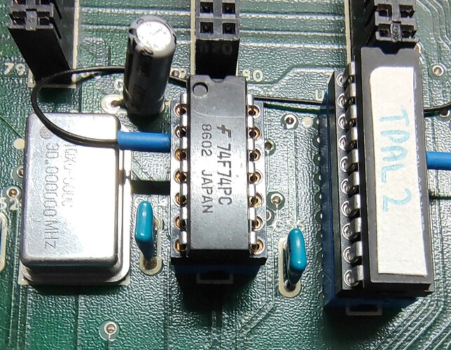
The diagnostics still failed. Once again, I proceeded walking through the guide and only right near the end did I spot my error. As I was walking through, I’d take the chips I’d removed and were supposed to put on the board aside. I got near the end and had a 74F74 instead of a 74LS74. I thought that was odd and reviewed all the 74F74’s that should be installed on the board.

Turns out the very first chip I put in the board, instead of being a 74F74, I inserted a 74LS74. This is hooked to the 30 Mhz oscillator that all the clock signals are derived from. It was just not quite fast enough to deal with the 30 Mhz clock signal, so none of the tests worked.

Pic of the offending chip, between the 30 Mhz oscillator and the TPAL:

Thinking this was the end of it, I proceeded onward, getting eventually to the video test.

I can see “something” occasionally, but it’s just not syncing. At this point, I suspect maybe the GBSControl simply wasn’t finding video mode I wanted properly (basically EGA), so I decided to download the latest version of the code and update my GBSControl.

Still the same thing. I suspect that it’s just not seeing the signal properly. I tried another monitor as well, but still no luck. From what I see from the monitor output, it just won’t do 15.7kHz @ 50 Hz,m and the GBSControl isn’t doubling that to 31.4 Khz.

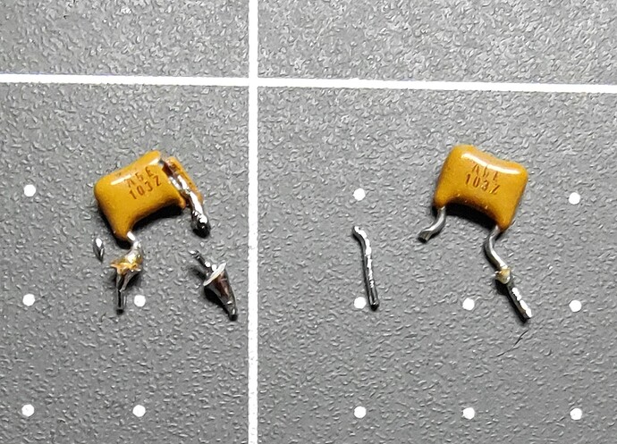
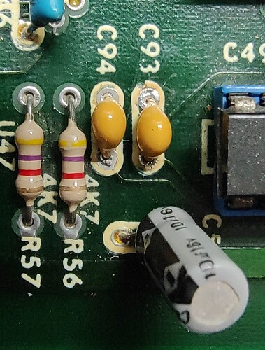
While looking over the board a second time, I noticed that a a lead on a small 56pf capacitor was broken. I also noticed the one next to it was broken as well.

Pic of broken caps:

Pic of caps replaced:

This however didn’t change anything with the machine working.

At this point I’m a bit stuck. It’s like things are running but the video is just not being decoded properly by the GBS Control. I don’t really have any other option (working) in the way of a screen at the moment. I have an IBM 5151 screen, but at the moment it’s in need of installation of some replacement caps (which I have), and a few parts of the case need a bit of work with some araldyte. That said, the machine it’s off (an IBM5160) still needs a lot of work so I could test the monitor. Also means if if something there doesn’t work, I won’t necessarily know what is at fault.

Also not 100% sure that the Applix1616 will drive the screen at the right sync rates. It supports mono, but nothing specific mentioned.

I’ll need to have a think about this. I might remove most of the chips and go at a much slower pace through the testing/build document again, especially now I’ve resolved the clock issues.

Will also reach out to some local (Canberra) people and see what options I have to borrow a suitable known working monitor.

1 Like

Update:

Now, I knew the Applix1616 had composite video, but it required making up a cable that goes on the standard DE9 connector (Pin 7 is the composite signal, Pin 1 is ground). So I decided to make up a cable and try it on the TV in our kitchen. The TV has a few dead vertical lines, but it does work and has composite in.

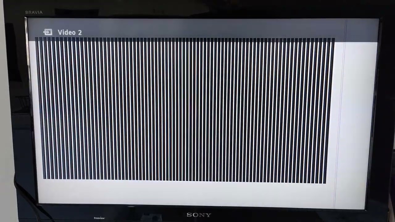
Lo and behold, the video test mode worked!

Video test screens (Video on Youtube):

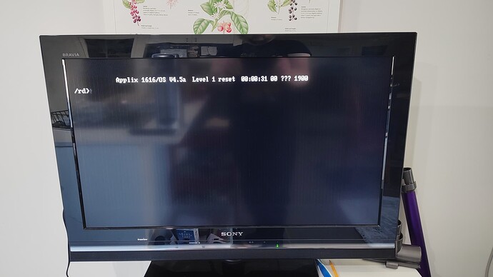
And when I changed the run/test switch, power cycled and then did a reset, I got the following:

Applix1616 Level 1 reset screen:

Based on that, looks like the ROMs are V4.5a. Of course, I’ll check that all once I get it properly running.

Note: I didn’t have a keyboard connected for this test. I think that I’ll come back to the Applix1616 tomorrow, give everything a once-over and then see where I can go from here.

4 Likes

Was looking at buying an RGB2HDMI previously, so with the need for a monitor option for this machine, and a guaranteed working monitor to test the IBM 5160 I also want to restore (which is MDA), I took the plunge and ordered one. I also ordered a TTL Buffer board, as I’d rather blow up a buffer board than the RGB2HDMI or a Raspberry Pi Zero. Have also arranged for a Raspberry Pi Zero to use with it from a local friend who has a few on hand. Don’t know if the RGB2HDMI will arrive before the end of the month though. Fingers crossed.

While I wait for an ETA on when it will arrive, I’m moving on to things I can do/solve in the meantime.

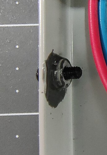
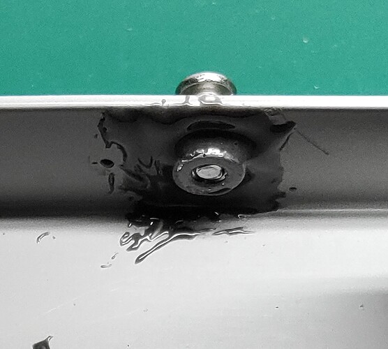
First up: The case top is held on with 4x 3mm screws. These were part of the case, but the embedded nut for one of these broke off. These look to be nutsert type rivnuts that were put into the case bottom, then possibly welded into place before painting. Getting hold of something similar here in Canberra might be a bit of a push, plus you usually need a special tool to insert them, so I’ll attempt to reattach it to the case.

Broke out the Permatex Cold Weld Araldite (designed for joining metal to metal) and glued it back in place. Used a nylon screw to hold it in place while it sets. The idea was that if the glue ends up on the screw, I can easily drill it out and remove any remainder from the hole.

Pic of glued embedded nut in side of the case:

This didn’t work as planned though. The join wasn’t as strong as I was hoping, and due to a someone previously trying to put the wrong screw into the case, the thread in the embedded nut was damaged. The nylon screw deformed enough to allow it to pass through the damaged thread, but when I attempted to put a proper steel screw in there, the pressure was too much for the join (which was not as good as I hoped) and the araldite failed.

I used a M3 tap to clean up the threads in the embedded nut. Will also be running the same tap through the other embedded nuts that are used to hold the lid in place as a precaution, as I would not be surprised if the threads are all damaged.

Once tapped, I cleaned up all the araldyte from the embedded nut and the case around the matching hole. Scratched up both surfaces heavily (with a pointed file) to give the glue more purchase. Using a steel screw and nut, pulled the embedded nut into place on the case as hard as I could. This actually made the embedded nut stay in the case without glue, though only loosely. I then Cold Weld araldyted the embedded nut to the case, while holding it with the metal screw/nut done up to keep it in place. I’m confident that the screw does not have any araldite on it, so it shouldn’t present any issues with removal.

Pic of screw and nut hanging from the embedded nut, but before araldite:

Pic of round 2 of using araldite on the embedded nut:

While I was waiting for the first araldyte join to cure, I proceeded to test what chips I can on the RAM/SCSI Expansion and the two Disk Controllers I have.

There were a few chip failures:

  • 1x Z80 on one of the Disk Controller boards.
    – Fortunately I have 2 of these boards, though the SCSI interface is only populated on one of them. Hopefully between them I can at least get one with SCSI working.
  • 7x KM44C256-8 RAM chips off the RAM/SCSI Expansion.
    – These are 256K by 4 bit wide chips. Lots of brands of these were made and used in a lot of things, but of course, getting hold of them may still be hard and even then you may end up with fakes.

I can’t test the NCR SCSI controller chips (NCR5380), and I’m yet to try ripping any of the PAL chips from the board, which will be next up. If any of the PAL chips are bad on the Disk Controllers, that may halt things.

I did however rip the Roms from the Disk Controllers (V1.4 and V2.2), and they all seem to be fine.

Pic of the boards with the bad chips removed:

I’m probably going to have to shelve the RAM/SCSI Expansion card for the moment and concentrate on one of the Disk Controllers. The SCSI access will be slow, but that is better than not working at all.

Reading the docs for the RAM/SCSI Expansion, it seems you need to load a driver off disk to be able to use the SCSI on that card. The main way they suggest you do this is to use the SCSI on the Disk Controller card to load the driver off the hard disk, then use the RAM/SCSI card for any remaining accesses. This means there’s 2 SCSI masters on the bus, both talking to the same drive. I asked one of the developers on the BlueSCSI Discord and they seem to think it should work fine with the BlueSCSI. Of course, the other alternative is to load the driver off floppy. I’ve got a Gotek floppy emulator that I could (in theory) load the drivers on, which would be more stable over time than using an actual floppy disk.

Thinking ahead to the next things to do:

  • There are a lot of holes in the back of the case, and they were how most of the dust got into the machine. Most likely, I will laser-cut some matching acrylic plates with the laser cutter at the Canberra Makerspace (aka Make Hack Void) to fill most of these holes. I’m also thinking I will put in an 80mm fan, since there is a suitable cut-out for one on the back of the case.
  • There are also holes in the bottom at the front for what most likely would be for a hard drive, either with brackets or directly screwing to the case. I might laser-cut some brackets or adapter plates for these as well, depending on what seems to be required.
3 Likes

Still no shipping info on the RGB2HDMI. Found some ram at a price I was willing to pay, but the earliest it’s supposed to arrive is October 30. If the ram turns up early, then I may take another look at the SCSI/RAM expansion card, though I’m not gonna get my hopes up.

Took the SPAL and ZPAL out of Disk Controller with the V2.2 ROM and ripped them. Decided to have a look at the RAM/SCSI Expansion PALs and noticed that apart from one 16R8, five of them are 20L8’s, and one is a 20R8. The ChipTester didn’t support 20L8/R8/R6/R4s PALs with the firmware I had on it (v3.4.2, latest at the time), but I put in a request with Evie at BackBit.io and in less than 24 hrs these were added to the latest firmware (v3.4.3), since they’re essentially the same idea as the 16L8/R8/R6/R4s just with more pins. The newer firmware logs details about L series PALs as well (which pins are mapped as inputs/outputs), so I’ve gone back and re-ripped all the PALs to collect all this info, beyond just the binary data.

FWIW: I really can’t overstate how satisfied I am with the BackBit.io ChipTester V2. It’s been a rock solid device and the support Evie provides is just amazing.

Also removed all the chips from that same Disk Controller in preparation for soldering/clean-up. I tend to leave chips in boards where possible unless I’m in the middle of something that requires their removal, as it’s too easy to accidentally bend a pin. This board was the one with the SCSI hardware/socket populated, but with a dead Z80. Time to solder up all the vias, then give it a clean and then check/touch up any joints that look in any way sub par, same as I did with the motherboard.

Bottom of board before soldering up all the vias/unused pads:

When I did all the vias, I also:

  • Fixed up the alignment on the molex connectors that power the floppies.
    – May replace these later. There’s 2 different types of connector here.
  • Realigned the 16 Mhz oscillator crystal, as it was sitting at an angle.
  • Installed M2 metal screws to hold the IDC sockets for floppy/SCSI onto the board.
  • Installed M3 nylon screws into the remaining blank holes that are for brackets and connectors.

Filling all the big holes with screws means less cleaner gets on the component side.

I also installed headers SJA-0 and SJA-1 for the Channel A onboard serial port. The serial ports hang off a Zilog Z8530 SCC connected direct to the Z80, allowing the Z80 itself to run serial operations, completely separate to the MC68000. It’s also apparently possible to use this for debugging the board. While I don’t have a spare Z8530 at the moment, populating the headers for Channel A at least is a no-brainer.

Of note: There are 2 sets of headers per serial port, on this board and also on the motherboard, all with the same pinout. For Channel A, they are SJA-0 and SJA-1. The SJ*-0 header is RS232 level and allows you to rewire the outputs to specific pins, including putting +12 and -12V power on specific serial pins. The SJ*-1 is TTL level and allows you to rewire specific outputs from the Z8530 to the RS232 level shifter IC’s (MC1488/MC1489’s). This means you can do things like loop back at the TTL level or the RS232 level just with jumpers, bypass a faulty input/output gate on one of the RS232 level shifters (if you have one unused), or tap off RS232/TTL serial from these connectors for all sorts of uses eg: directly to other devices, implement different serial types like RS422/423, have connectors located elsewhere on the case, etc.

Top of board after soldering up all the vias/holes, but before cleaning:

Once again, cleaned the board with Servisol Circuit Board Cleaner NA-1008.

Bottom of board after cleaning, prior to fixing joints:

Close up pic of some of the joints (around the Z80 socket):

Things to do next:

  • Now that I can actually see all the existing joints, time to fix them all up.
  • Perform a raft of continuity tests around the Z80 and compare to the other Disk Controller board, where the Z80 was fine.
    – Definitely don’t want to plug my remaining Z80 into this board and kill it.
  • Go through the some of the comissioning tests (hopefully).
2 Likes

Short weekend update:

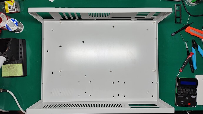
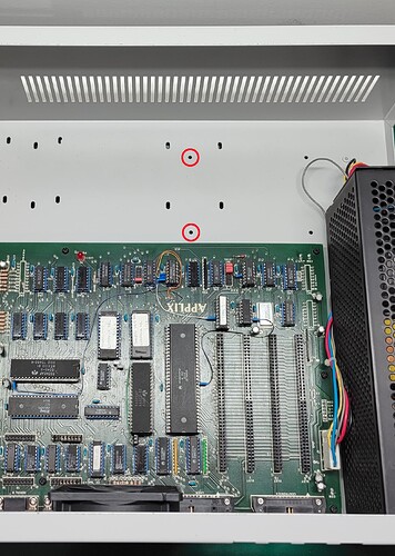
Was looking at how to mount the BlueSCSI and found that 2 case holes right in front of the motherboard are exactly 68mm apart, which just so happens to match 2 of the holes in the BlueSCSI V2 Desktop. There’s also just enough room between the BlueSCSI and the Motherboard for everything to fit nicely. As long as I use the shortest nylon stand-offs I have, any cards in the motherboard slots should clear the top of the BlueSCSI easily. I’ll put a 3rd standoff on the BlueSCSI but not screwed into the case so that it doesn’t wobble on just the 2 stand-offs.

Inside of case with holes circled in Red:

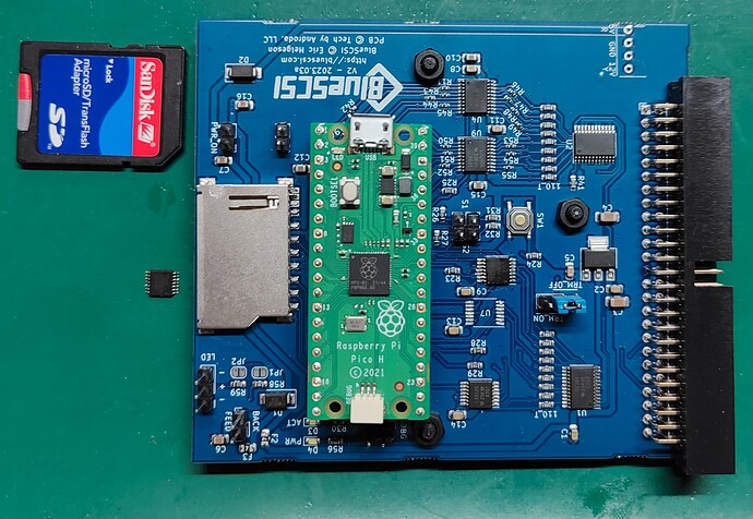
That said, while setting up the the BlueSCSI V2 Desktop with mounting posts ready to go into the case (just after installing the latest firmware), I noticed that one of the chips fell off the BlueSCSI board.

BlueSCSI V2 Desktop with the chip that fell off (U7) sitting next to it:

Have contacted the supplier on Saturday afternoon by email, and they got back to me in a few hours. Going to send it back to them on Monday. They’ll sort it out then get it back to me, no charge. Fortunately they’re in Sydney, so turn-around won’t be too long. It was supplied as a kit (with all the SMD parts already mounted on the board), so it’s hard to test till it’s assembled. Very happy with their service to resolve this, though of course any delay is not ideal.

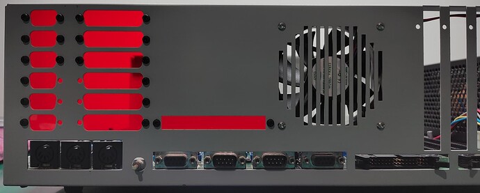
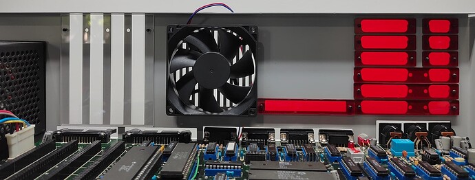
Cut some of the patching plates on the laser cutter at Canberra Makerspace today and tapped them for M3 screws. Mounted them on the case and used nylon screws as I’m still low on the original screws. Also put an 80mm fan in the case as well. The plates are 3mm red acrylic, which I found in the scrap bin at the Makerspace. The red is very similar to the 1616 in the Applix logo, so it seems to go well with the case.

Back of the case with the plates installed:

Cut a plate to cover up the card slot holes (since the cards don’t have brackets on them), but I got the holes in the wrong place, so will need to give it another go.

There’s a place for a 6 pin header on the motherboard (near the power connector) that has GND, +12V, -5V, -12V, +5V and GND (repeated) on it. I should be able to run the fan off the GND and +12V pins. If needed, I could run the BlueSCSI off the +5V and GND pins, though in theory the BlueSCSI should be able to work on the SCSI bus termination power.

May also have a suitable monitor coming to me. Just waiting to find out when I might end up with it.

1 Like

Touching up the soldering on the Disk Controller has evolved into using my vacuum desoldering station to remove a lot of probably bad solder from the board. :frowning_face:

When I tried touching up the soldering around the sockets, there were a lot of joints that just didn’t want to take solder well. I switched to doing all the passives (caps/resistors/headers) and apart from the big 80 pin header on the board edge, most of these went fine and didn’t require any extra work.

My guess is that the person who assembled this board ran out of solder during the assembly (possibly while doing the 80 pin expansion connector) and switched to a different roll, which was contaminated in some way. As a result, I’m removing most of the solder, particularly from the sockets, using my desoldering station and will reapply new solder. Note that I’m just aiming to remove the existing solder. I’m not deliberately trying to remove any sockets from the board, so I don’t need to make sure I’ve removed all the solder from a joint. Just enough to allow me to make a new good clean solder joint. That said, a lot of them are coming off (and a socket pin fell out of one of them), so I may just replace many of the sockets with new ones, since I have some on hand. The blue sockets look nice on the board, but I’d much rather have working sockets.

Part way through some desoldering:

Some desoldering station tips:

  • Hold the PCB at right angles to the table, rather than leaving it flat on the table.
    – This way, you’re not fighting gravity to pull the solder out of the joint/board. You’re just pulling the solder out of the joint/board.
  • Put the nozzle over the joint, wait for it to melt, pull the trigger. Once you’ve sucked away the solder, pull the desoldering gun away from the board before releasing the trigger. I usually release the trigger about 1/3 to 1/2 second after removing the gun from the board.
    – This allows the nozzle and barrel of the desoldering gun to clear properly, since it should no longer be blocked by the board/component/joint, allowing more pressure to pull any remaining solder in the gun through the barrel. It also helps avoid the back half of the gun barrel (which is colder) clogging with solder, which is a right pain to clean out.

Over 100 joints worth of solder out of my desoldering station (after cleaning):

Just a note on my desoldering station:

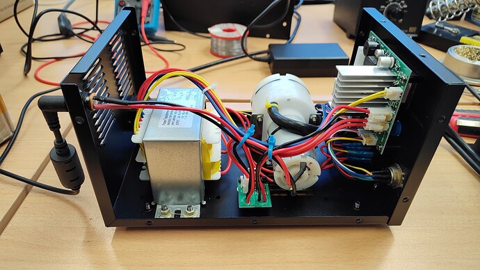
I’m using a Yihua 948-I desoldering station, but I’ve modified it slightly. The pump motor in these gets run through a somewhat odd driver circuit that limits the max voltage to about 10.5V. As a result, the suction isn’t very great, which is a well known problem with these units. The actual pump motor is normally rated at 12V, and can be run up to about 14V without it causing too much of an issue (listed as 9-14V).

There’s no feedback circuitry on the motor (eg: stall detection), so I’ve made up a small board that is mostly just an opto-coupler and a MOSFET, so that I can use the existing motor output to drive the motor from an external supply connected to a barrel jack on the back of the unit. Running it at 12V provides a fair bit more suction than the default, and if I wanted I could make the voltage slightly higher (eg: 14V). I did look to see if I could power it without an external supply, but the built in transformer simply can’t supply the power, even if you use a voltage boost circuit.

I only made 5 of these boards (JLCPCB for the PCBs and used components I had on hand), and I’ve given 2 away already. There’s not much to it (opto-coupler, diode, 3 resistors, MOSFET and a bunch of connectors). There seems to be a bit of interest, so I might spin up a V2 with more commonly available components and put it up somewhere.

Inside of the Yihua 948-I with the first version of the little driver board installed to the left of the pump motor:

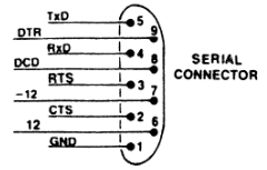
During breaks in desoldering, I’m reviewing the circuit diagrams (as limited as they are) for the motherboard, disk controller and memory/SCSI expansion, so I have a better idea how things sit together and what sort of basic tests I can perform on boards before I even get to powering the disk/memory boards up. During one of these reviews, I noticed that the DE9 serial connectors on the back of the Applix motherboard and on the Disk Controller are NOT the standard wiring for DE9 serial!

Applix DE9 serial connector wiring:
Applix1616 DE9 serial port

Of the various types of null modem cables I have (I have lots), one would have shorted +12V to -12V, while another would have shorted +12V to Ground, and a third would have shorted -12V to Ground. None of these outcomes would be useful at all!

So what I’m most likely going to do is:

  • Cap off these connectors (with some plastic covers that screw over the socket) so nothing can be inserted in them without deliberately removing the cover.
  • Make some cable harnesses that connect the 2x9 way headers (SJ*-0) to correctly wired serial connectors, which I’ll then mount on the back panel.

This will mean some of the plate covers I laser cut will not actually be needed, but that’s not a huge problem to have. That said, I might be able to repurpose them as part of the cover to block the existing ports, at least until I sort out something more long-term like a 3D printed cover or removing the on-board serial sockets altogether.

On the monitor front, I hopefully should have an RGB CRT monitor in my hands either late this week or early next week. I’ve still got the RGB2HDMI on the way, but it’s coming from the US and UPS has still not picked it up from the supplier.

As for other peripherals, the Applix1616 uses an XT keyboard. It won’t work with an AT one, unless it has a switch to support XT. I have 2 possible keyboards I can try.

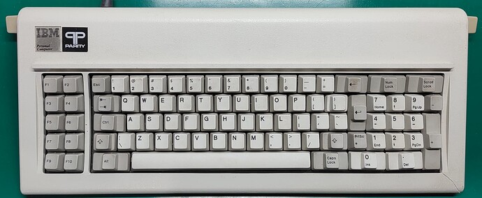
The first I one have is a genuine XT keyboard (the Model F off my IBM 5160). The case is cracked in 2 places (right front corner and the bar between the F10 and Alt keys) and I don’t know for sure if it is electrically sound. So that’s the next thing I’ll be tackling, which apart from repairing the case and confirming the insides are OK, will involve giving the keyboard power and using a cheap logic analyser to see if it generates the right clock/data signals when keys are pressed.

IBM Model F keyboard with cracked case:

The second keyboard is a switchable XT/AT keyboard. When I tried this with the Applix originally, it didn’t seem to work, so I am going to perform the same test on it as well. Hopefully one of these keyboards will work, else I’ll have to see what else I can find.

For reference on the differences between XT and AT keyboards: DOS Days - XT and AT Keyboards

2 Likes

After removing all the dodgy solder (and therefore all the sockets) from the Disk Controller, I did some tests on the board and found a low resistance (31 ohms) between +5V and Ground. For reference, the other almost fully populated board is about 5k between +5V and Ground, though it doesn’t have the SCSI termination resistors (this is a hint).

Turns out, this was just the SCSI termination resistors. Each one puts 550 ohms (330 ohms and 220 ohms in series) between 5V and Ground, and there are 18 of them (9 per resistor pack, 2 packs in series). That works out to about 30.5 ohms.

Not realising this and then chasing it cost me just over an hour. :grimacing:

As part of this, I removed a bunch of electrolytic caps, some of the ceramic caps, and the SCSI termination resistors.

All the sockets gone and some components lifted:
[

All is not lost here though, as the board looks much cleaner and I’m now 100% sure everything is fine. I’m also going to put the SCSI termination resistors in machined sockets, which I’ll need to go buy, since I don’t have any on hand. This means if I need to put more than one SCSI terminated device on the bus (eg: 2 SCSI controllers), I can just remove the resistor packs from this one without doing any more desoldering.

Anyway, I then proceeded to solder on all the sockets. Everything looks MUCH nicer. I used machine sockets for the NCR5380 (SCSI) and the Z80, the MC1488/1489 serial driver chips, the WD 1772 floppy controller and also some associated floppy drive circuitry. Part of this was so that they’re less likely to be an issue if I need to replace these (as most are related to off-board interfaces like SCSI/floppy/serial ports), but it’s also because I ran out of standard 14 and 20 pin IC sockets. I’ve still got all the old blue sockets, but I’d rather not use them, at least till I properly check them out.

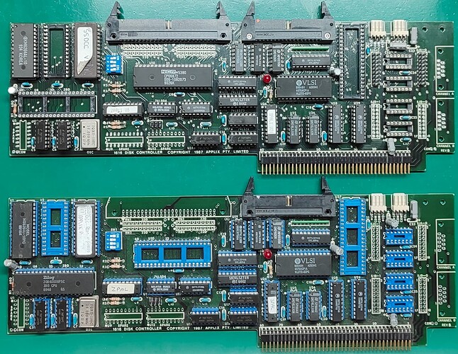
Tops of both boards next to each other. Blue sockets on the V1.4 board, black sockets on the V2.2 board:

Note that I also replaced all the off-board power connectors on both these boards with some I had on hand from my 3D printer building days. They’re not the standard 4 pin floppy connectors, but then neither where the originals, and they actually match the connectors on the cables.

Plan next on these is to install a 50 pin header on the V1.4 board (normal, not with the retaining clips) and machined sockets for the resistor networks on both boards. I should then be able to use either board for SCSI.

Note: To use the V1.4 board with SCSI, I will need to install the V2.2 Rom and just to be safe will also swap over the PALs. The V2.2 Rom has all the code for driving the SCSI side of things, whereas V1.4 does not.

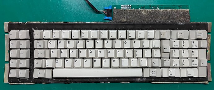
With that done, I moved onto the IBM XT Model F keyboard. I opened it up and confirmed that the PCB looks intact. I removed all the crud under the keys before taking a photo. It was quite rank, and no one wants to see that.

PCB and keys on the inside of the XT Model F keyboard:

The Model F keyboard is weighty. The reason for this is that the steel plate (which appears to be phosphor bronze coated) which is behind the keyboard mechanism is 1.6mm (or 1/16") thick, and the plate itself is roughly 13x44cm (curved to shape), which is about 91.5 cm³ in volume. Assuming it’s steel, that’s roughly 720 grams just by itself (based on 1m³ of steel being roughly 7900kg). That doesn’t even include the plate all the keys are mounted on. The plastic of the case is somewhat fragile from age, so even a light drop could cause it to crack/break, which appears to be what happened here.

I’ve put the case aside for the moment. All the bits are there, the mechanism is intact and the cracks should be fine with some araldite, but if the insides don’t work, I’m not going to spend the effort on repairing it at this time.

Now I don’t have any 5 pin DIN sockets, but fortunately the Model F has a 10 pin IDC connector for the keyboard cable on the inside. It also has 10 matching pads, 4 of which are connected to the 4 pins used in the XT keyboard cable. I’m assuming this was a pogo pin location used for testing the keyboard in a jig.

Close up on the test pads (silver squares) and the connector (blue/black):

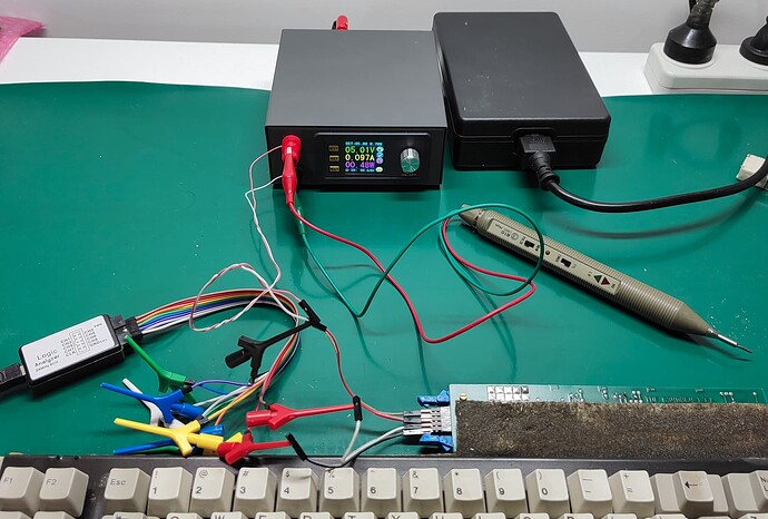
Fortunately I do have a 10 pin IDC connector that will fit on the pins in that socket, so I wired up a test system so I can power the keyboard from 5V and then watch the clock/data lines on my cheap digital logic analyser.

So I traced back the pins on the DIN cable and came up with the following wiring:

1 - Black - Clock
2 - White - Data
3 - NC
4 - Red - Ground
5 - Brown - +5V

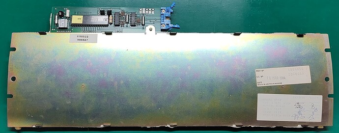
Now I always worry when something like Red is the Ground, so I went and looked up the schematic for an XT Model F. There’s a 40 pin IC on the board (underside of the piece that sticks out the top). Pin 20 on the IC is Ground, while Pin 40 is 5V. Used a multimeter to confirm that Red was indeed Ground before proceeding.

Bottom of the XT Model F keyboard, showing the steel plate and the 40 Pin IC:

Wired up a power supply (set to 5V) and then checked I was getting signals on Clock/Data using a logic probe, which was a good first sign and meant the wiring was working. I then hooked the keyboard up to my little logic analyser.

All hooked up to my Saleae-clone 24 Mhz logic analyser, which was not plugged into a PC at this point:

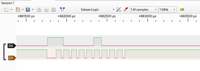
Everything looked good. With power on, the keyboard was drawing just under 100mA, which is good and well within spec for the Applix. Fired up PulseView (I use Sigrok under Linux, using the fx2lafw driver for this device) and took a capture.

Screenshot from PulseView. D0 is Data, D1 is Clock:

So the keyboard works! Now I should be able to use it on the Applix. Will only need to fix the case to restore it to being fully functional.

Speaking of cases, I laser cut a new blocking plate for the slots at the back of the Applix. I don’t normally get into the Canberra Makerspace on a weeknight, but last night was the AGM. Since I was there, I jumped in before the AGM to cut the revised version of the plate out of 2mm clear acrylic. Clear was all I had available in 2mm, as I think 3mm may be too thick and collide with the expansion boards.

Pic from inside the case looking at the back:

Next up:

  • Repair the IBM XT Model F keyboard case.
  • Finish up the Disk Controller boards.
  • Check/test floppy drives.
4 Likes

Hi Stuart,
Great to read about your Applix 1616 restoration… certainly brings back lots of fond memories.
I have three 1616s which I’ll get around to restoring at some point.
The first one is my original personal 1616 which is the first prototype PCB we got back. It pretty well worked except for compatibility issues with some keyboards and VIAs, hence the pull-ups on the 6522.
The second one was used by ANSTO and was given to me as a gift by a friend of mine about 10 years ago.
Both these are the original 8Mhz 68k with the Z80 disk controller.
The last one was given to me a couple of years ago and is pretty well the same as the one you are restoring.
Glad to see the PAL’s you have are readable and can be copied. Unfortunately I don’t have the master PALs so was a little worried about this. All the early PALs were not copiable, as we didn’t want our masterpiece ripped off lol.
Anyways, super excited to see your progress
Have fun :slight_smile:

Paul Berger

Hi Paul,

Great to hear from you.

I asked the person who produces the ChipTester about the format the PALs are read as, and it seems it’s producing brute-forced bit dumps (in a .bin format), which I’m not sure are going to be useful. They definitely won’t contain any logic formulas. Looking at a few shows some data, but in some cases it’s just the same byte repeated over and over, which doesn’t seem promising.

It’s good to hear there’s more of these units out there.

So haven’t done a huge amount due to unforeseen personal circumstances that I won’t really go into here, except to say that it’s made a bit of an emotional impact over the last few days that has left me drained.

Managed to get my hands on an old Taxan SuperVision IV CRT monitor. It didn’t come with a cable (which I was hoping for), so I had to make one.

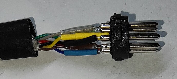
The Taxan screen takes RGB video in on a DIN 8 pin socket on the back, so needed to wire up a DE9 connector to a DIN 8 pin plug suitable for the RGB input.

Din plug end:

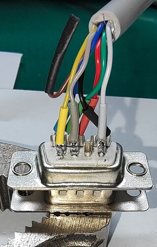
DE9 end:

As the wires are quite thin, the insulation tends to shrink back even with just a small amount of heat. I used heatshrink on the wire before soldering to the connector to help avoid this being an issue. If the insulation shrinks back too much and the wires bend, you can get a short.

Note: The brown wire isn’t connected at the DE9 end, but I didn’t want to cut it out of the cable, just in case I need it later, so I put a bit of heatshrink over it to keep it isolated from everything else.

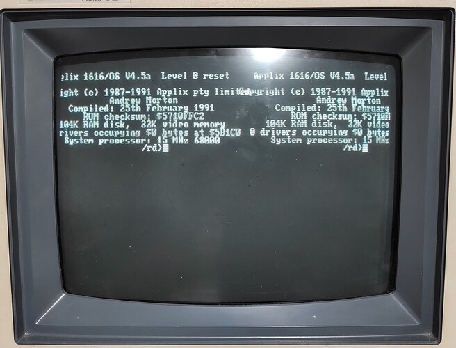
After all this, it seems the screen doesn’t like the horizontal sync rate, leading to a sort of “on-screen duplication”. This is better than all the LCD monitors and another CRT I have, but still sub-optimal. I have confirmed that the signals out of the video connector are on the right pins, the wiring for the cable is correct and the cable is actually wired that way. the monitor has a set of dip switches on the back for various formats, including inverting the sync, but none of this helped.

Duplicated text due to incompatible scan rate:

One thing that came out of this though is that I found out that the KBD jumper on the motherboard needs to be bridged to work with the IBM XT Model F keyboard. No pins were installed on the board, so I installed header pins on that spot then put a jumper on them. While I had the motherboard out, I installed a 6 pin header on the power connector.

New 6 pin header near the power connector and 2 pin KBD connector with jumper:

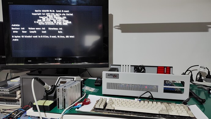
At the moment, I’ve gone back to the old TV, since it actually gives me output (composite), even if it’s only Mono. This does require selecting a different output and then switching back to the Applix to get a display though. Note that I did try using the GBSControl with the VGA input on the TV, but that had the same issue with sync that almost every other monitor has. As such, I’ll still need to wait on the RGB2HDMI to use it on a reasonable LCD monitor in colour. According to USPS, that’s still in the US, so I suspect that might arrive after the end of the month.

Keyboard now works, though sometimes you need to unplug/replug it to reset it on boot. Once it works, everything is good.

Machine on the desk with working keyboard and using composite video output:

Did some very basic electrical tests on the floppy drives, and neither seems to be problematic.

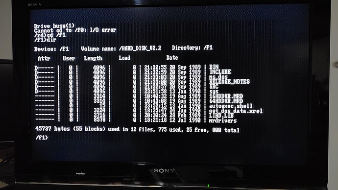
Hooked up the V1.4 card (floppy only) and one drive to see what we get.

And it works! I used the “Hard Disk Update” disk that came with the machine and it was happily reading it.

The floppy drive eject mechanism on both drives isn’t fully ejecting the disk. It lifts the disk to clear all the internal parts of the mechanism, but doesn’t successfully push the disk out, so you need to manually pull it out. I’ll take a look inside the drives at some point to see if this is something simple like gummy grease on the mechanism, or something more complex.

Some Floppy disk notes:

  • Tried using some RAW image files that others have recovered directly from Applix floppies in a GoTek, and the Applix kept complaining about disk errors. I just renamed them .IMG from .RAW, so it’s possible they’re in the wrong format.
  • While looking further into things, I probably need to flash the GoTek with something like FlashFloppy+ GitHub - keirf/flashfloppy: Floppy drive emulator for Gotek hardware but I don’t have a suitable way to do this currently (USB-A to USB-A or TTL Serial to USB cable for programming). Will see if I can do this with some equipment at the Canberra Makerspace.
  • All the disk images are 720K. I have a Greaseweazle V4 that a friend is currently borrowing that I might get back and see what it makes of the (working) disk I have. It’s possible that the raw images need to be manipulated to work, and this should allow me to get a known working image off the disk to test/experiment with in the GoTek (whether using FlashFloppy firmware on the GoTek or not).
    – Just FWIW: Greaseweazle and FlashFloppy are both developed by the same person.

Other things:

  • Haven’t yet heard back about my BlueSCSI V2 Desktop repair yet.
  • Ram looks like it may have left China, but nothing confirmed.
2 Likes

Excellent progress! Soldering those DIN connectors is such a pain.

With Flashfloppy firmware on your Gotek, use HxCFloppyEmulator to convert your RAW/IMG images to HFE format and then they should boot.

1 Like

Thanks ChickenMan, that’s great to know. I’ll need to see if I can run that in Wine or something, cos I don’t tend to have Windows machines about. Pretty sure there’s a bunch of other tools that can do the same thing (to HFE) though that do work natively on Linux.

FWIW: I managed to get FlashFloppy+ on the GoTek (found I had a USB to TTL Serial adapter about). Will go through the details in a later post.

1 Like